Acoustically Mapping IGBT Module Solder Thickness
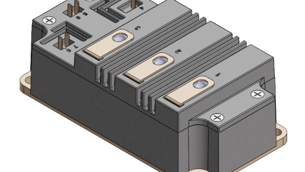
Previously, a Power Electronics Technology article titled “Inverted Acoustic System Cuts IGBT Failures” (September 2011) examined the use of an acoustic microscope to image heat-blocking defects such as voids and non-bonds in the solder typically used to bond a heat sink to the bottom side of an IGBT module. Finding these defects makes it possible to remove them from assembly and to rework modules whose total void and non-bond area may cause the die to overheat and fail.
The transducer of an acoustic microscope typically scans the surface of an IGBT module’s heat sink, pulsing ultrasound into the module and receiving echo signals from material interfaces at various depths. Medium-amplitude echo signals come from interfaces between solid materials. The highest amplitude echo signals come from the interfaces between a solid and a gas (generally air), at a defect boundary such as a void or a non-bonded interface.
A technique recently developed by Sonoscan permits the microscope operator to evaluate the thickness of the solder layer at the same time that the IGBT module is being scanned to find voids and other anomalies. The Time Difference Mode used with Sonoscan’s C-SAM® acoustic microscopes evaluates the thickness of the solder at every x-y coordinate into which the scanning transducer pulses ultrasound. The transducer pulses ultrasound into thousands of coordinates per second. The resulting acoustic image is a detailed map of solder thickness across the IGBT module.
Time Difference Mode
The key events in the Time Difference Mode are these:
When ultrasound is pulsed by the transducer into the heat sink, the ultrasound travels though the heat sink and is partly reflected at the material interface where the heat sink meets the solder.
If the heat sink and the solder are well bonded at the interface, the return echo will have a moderate amplitude, resulting in a gray pixel in monochrome imaging. (The precise amplitude and gray level can be predicted from the characteristics of the two solid materials.)
If a pulse strikes the interface between the heat sink and a gap-type defect – i.e., between metal and air – essentially all of the pulse is reflected to the transducer at very high amplitude. The pixel is bright white.
When the echo arrives at the transducer, the elapsed time since it was launched is measured in nanoseconds. The time is converted into distance to measure solder thickness.
After a pulse is launched from the transducer, echoes may arrive from all interfaces in a sample, and at different times. For this reason, a technique called gating is used to avoid uncertainty about the depth of a particular feature. Return echoes are gated on the depth of interest, meaning that only echoes reflected from features within the depth of interest are used to make the acoustic image. These echoes arrive at the transducer within a specified time after the launch of the pulse. Echoes arriving before or after this time are ignored. In the imaging of the IGBT module solder layer, echoes are gated from a depth just above the top of the solder layer to a depth just below the bottom of the solder layer.
In commencing the imaging of an IGBT module, or any other sample, the operator sends a series of pulses into a single x-y location and collects the return echoes to get an idea of the depth and amplitude of echoes from major material interfaces in the sample.
The results of this interrogation are displayed as a waveform (Fig. 1). These waveforms are from ultrasound pulsed into two different x-y locations on the heat sink of the same IGBT module. On each waveform, the surface of the heat sink is at left. Two downward spikes are marked by the yellow lines. The spike at left is the interface between the heat sink and the solder. The spike at right is the interface between the solder and the substrate, which in this module is a ceramic piece. The time difference between these two interfaces is measured and converted into distance to measure the solder thickness. The difference in solder thickness at these two locations is significant.
Spikes to the right of these features mark interfaces (die attach, for example) farther into the module. Two vertical lines (not shown here) are moved horizontally to set the gate – i.e., to define precisely the upper and lower limits of the depth from which echo signals will be used for making the acoustic image.
Creating waveforms for two x-y locations only tells the solder thickness at two of the millions of x-y locations that the transducer will scan when imaging the sample, but it helps the operator select good locations for the gate limits.
Fig. 2 shows in diagram form what happens when the transducer scans the top of the heat sink and pulses ultrasound downward into the module. The two solid-to-solid material interfaces (heat sink to solder, solder to substrate) will send back medium-amplitude echoes, as shown in Fig. 2, and will appear gray in a monochrome acoustic image.
If there is a gap-type defect such as a void in the solder, the gap will send back echoes of the highest amplitude and will appear bright white in a monochrome acoustic image. A void may occupy the whole thickness of the solder, or it may be much thinner and may lie at any depth within the solder. What matters is the solid-to-air interface at the top of the void, from which >99.99% of the pulse is reflected, no matter how thin or thick the void may be (as long as it is thicker than 0.01 micron).
At each of the millions of x-y locations from which the transducer collects echoes, the echo from the heat sink-solder interface (A in Fig. 2) will arrive at the transducer a fraction of a microsecond before the echo from the solder-substrate interface (B in Fig. 2). The Time Difference Mode converts the difference in arrival times into distance to indicate the thickness of the solder at that x-y location. At the end of the scan, the acoustic image can display thickness as a variably colored background map on which voids and other gap-type defects are seen as discrete features. Typically, the operator will produce two images, one to display defects, and the second to display solder thickness. The second image will also display defects in the solder.
Fig. 3 is the Time Difference Mode acoustic image of one portion of a large multi-die IGBT module, imaged from the heat sink side. The ceramic pieces and the die are thus below the heat sink; it is the near side of the ceramic pieces that forms the rectangles seen in the image.
This image displays solder thickness rather than the acoustic reflectivity of each feature. The thickest areas solder are pink, while the thinnest areas are orange. Most of the numerous irregularly shaped voids in the solder are red, not because of their high reflectivity but because they are very close to the top of the solder and the Time Difference software measures the distance from the top of the solder to the top of the void. Some smaller voids deeper in the solder are blue.
The solder in the unit at the far left is thicker toward its right edge (pink) and much thinner toward the left edge (orange). The cause of the variation in the thickness of the solder may be a tilted ceramic piece beneath the solder. Near the left edge is a black band, which probably indicates an area where the solder is extremely thin or even absent.
In Fig. 4, the same portion of the module is again imaged by the Time Difference Mode to measure solder thickness, but in this image a color map having non-adjacent colors was used in order to make clear the distinction between accept and reject.
Graphic Representation
The color map is shown above the Time Difference image. Colors at the right are thicker; those at the left are thinner. Each color represents a thickness increment of 45 microns. Black, at left, represents a thickness range of 0 to 45 microns, while white, at right, represents a thickness range of 495 to 540 microns. A good IGBT module would display a few colors near the center of map, and the total thickness range would be modest. This Time Difference image includes black (thinnest solder) and, in tiny areas, dark green. It does not include white (thickest solder) or magenta, but does include (at the extreme right of the leftmost tile) dark blue. The maximum thickness range is therefore nominally from 0 microns to 450 microns. Overall, the thickness image of this portion of the IGBT module does not suggest high reliability.
The introduction of the Time Difference Mode means that a C-SAM acoustic micro imaging system can, in a single scan through the heat sink, image the voids and other defects in the solder, computer the total area of these defects, and create a color map that shows which areas of solder thickness are within spec and which areas are not.
Established in 2004, Coding International Co., Ltd (shenzhen Coding Technology Co.,Ltd) is a gather the development, production, marketing combine together of the semi-conductor professional company. We can provide a wide range of capabilities in research and production such as all kinds of Diode, Triode transistor, Audions, Triac, Dynatrons, Thyristor, LED product, Optocoupler, Silicone Bridge, IGBT power Module and Surge arrester, ICs, ect.
This article by blogcoding original compilation, please indicate the source:http://www.codingintl.com/blog/1143.html


Post a comment